- 您现在的位置:买卖IC网 > Sheet目录243 > PRTR5V0U2K,132 (NXP Semiconductors)DIODE ESD PROTECT R-R DBL SOT891
NXP Semiconductors
PRTR5V0U2F; PRTR5V0U2K
Ultra low capacitance double rail-to-rail ESD protection
1.4 Quick reference data
Table 2. Quick reference data
T amb = 25 ° C unless otherwise speci?ed.
Symbol
Parameter
Conditions
Min
Typ
Max
Unit
Per channel
C (I/O-GND)
input/output to ground
f = 1 MHz;
-
1.0
1.5
pF
capacitance
V (I/O-GND) = 0 V
C (I/O-I/O)
input/output to input/output
f = 1 MHz;
-
0.6
-
pF
Zener diode
capacitance
V (I/O-I/O) = 0 V
V RWM
reverse standoff voltage
-
-
5.5
V
C sup
supply pin to ground
f = 1 MHz;
-
16
-
pF
capacitance
V CC = 0 V
[1]
[2]
[3]
Measured from pin 1, 3, 4 or 6 to ground.
Measured from pin 1 or 6 to pin 3 or 4.
Measured from pin 5 to ground.
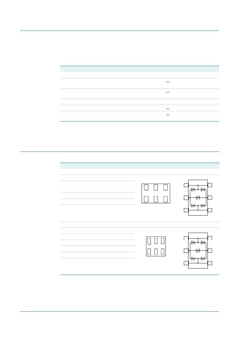
2. Pinning information
Table 3.
Pinning
Pin
Symbol
Description
Simpli?ed outline
Graphic symbol
PRTR5V0U2F (SOT886)
1
I/O1
input/output 1
2
GND
ground
1
2
3
1
6
3
I/O2
input/output 2
4
5
I/O2
V CC
input/output 2
supply voltage
2
5
6
I/O1
input/output 1
6 5
bottom view
4
3
4
006aab349
PRTR5V0U2K (SOT891)
1
I/O1
input/output 1
2
GND
ground
1
2
3
1
6
3
I/O2
input/output 2
4
5
I/O2
V CC
input/output 2
supply voltage
2
5
6
I/O1
input/output 1
6 5
bottom view
4
3
4
006aab349
PRTR5V0U2F_PRTR5V0U2K_2
? NXP B.V. 2009. All rights reserved.
Product data sheet
Rev. 02 — 19 February 2009
2 of 12
发布紧急采购,3分钟左右您将得到回复。
相关PDF资料
PRTR5V0U2X,215
DIODE ESD PROTECTION SOT143B
PRTR5V0U4AD,125
DIODE ESD USB SC-74
PRTR5V0U4D,125
DIODE ESD USB 6-TSOP
PRTR5V0U4Y,125
DIODE ESD PROTECT SOT-363
PRTR5V0U6AS,118
DIODE ESD PROTECTION 8-SOIC
PRTR5V0U6S,118
DIODE ESD PROTECTION 8-SOIC
PRTR5V0U8S,118
DIODE ESD PROTECTION 10-TSSOP
PS-11279
BOX ABS 6.3" X 3.75" X 1.41"
相关代理商/技术参数
PRTR5V0U2X
制造商:NXP Semiconductors 功能描述:DIODE TVS DUAL SOT-143B 制造商:NXP Semiconductors 功能描述:DIODE, TVS, DUAL, SOT-143B
PRTR5V0U2X,215
功能描述:ESD 抑制器 5.5V DUAL R-R ESD ULTRA LOW CAP RoHS:否 制造商:STMicroelectronics 通道:8 Channels 击穿电压:8 V 电容:45 pF 端接类型:SMD/SMT 封装 / 箱体:uQFN-16 功率耗散 Pd: 工作温度范围:- 40 C to + 85 C
PRTR5V0U2X,215-CUT TAPE
制造商:NXP 功能描述:PRTR5V0U2X Series 9 V 16 pF Rail-to-Rail ESD Protection Diode - SOT-143B
PRTR5V0U2X215
制造商:NXP Semiconductors 功能描述:TVS-DIODE
PRTR5V0U4AD
制造商:PHILIPS 制造商全称:NXP Semiconductors 功能描述:Integrated quad ultra-low capacitance ESD protection
PRTR5V0U4AD T/R
功能描述:TVS二极管阵列 DUAL USB 2.0 ESD PROTECTION RoHS:否 制造商:Littelfuse 极性: 通道:4 Channels 击穿电压: 钳位电压:11.5 V 工作电压:2.5 V 峰值浪涌电流:20 A 安装风格:SMD/SMT 端接类型:SMD/SMT 系列: 最小工作温度:- 40 C 最大工作温度:+ 85 C
PRTR5V0U4AD,125
功能描述:TVS二极管阵列 DUAL USB 2.0 ESD RoHS:否 制造商:Littelfuse 极性: 通道:4 Channels 击穿电压: 钳位电压:11.5 V 工作电压:2.5 V 峰值浪涌电流:20 A 安装风格:SMD/SMT 端接类型:SMD/SMT 系列: 最小工作温度:- 40 C 最大工作温度:+ 85 C
PRTR5V0U4AD125
制造商:NXP Semiconductors 功能描述:DIODE ESD USB SC-74
